Designing VdW Quantum Materials
Unlike materials synthesized through conventional growth methods, heterostructures mechanically assembled from 2D materials are held together by the van der Waals force and do not necessitate matching chemical properties or lattice parameters among adjacent layers. Thus, it allows the creation of an infinite variety of new material structures, bounded only by the limits of our imagination. We draw layers from the extensive 2D material repository and engineer their stacking to create desired quantum properties.
At the heart of this rational design approach lies the interplay between 2D layers across atomic interfaces. In the past, we have harnessed Coulomb attraction across atomically thin insulators to craft a novel superfluid—the exciton condensate. Additionally, when adjacent 2D layers have mismatched or misaligned lattices, a larger moiré periodicity emerges, defining an artificial lattice and giving rise to entirely new properties, including flat bands, strong correlation effects, and exotic topological orders. We look forward to embrace and integrate these cross-layer interplays to explore the uncharted territory of quantum matter, ranging from unconventional condensation to quantum spin liquids and topological superconductivity.

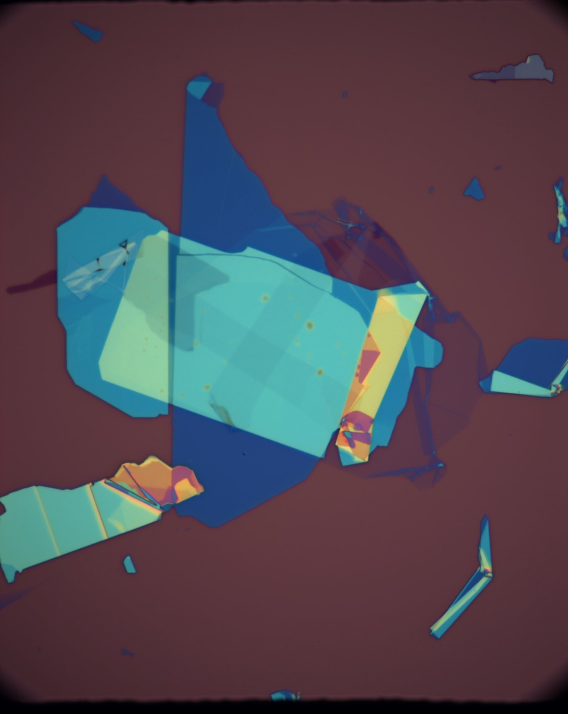
A vdW heterostructure.

A nano-fabricated vdW device.

A vdW device ready for low temperature measurements.

Interlayer fractional quantum Hall effect. Nature Physics (2019)
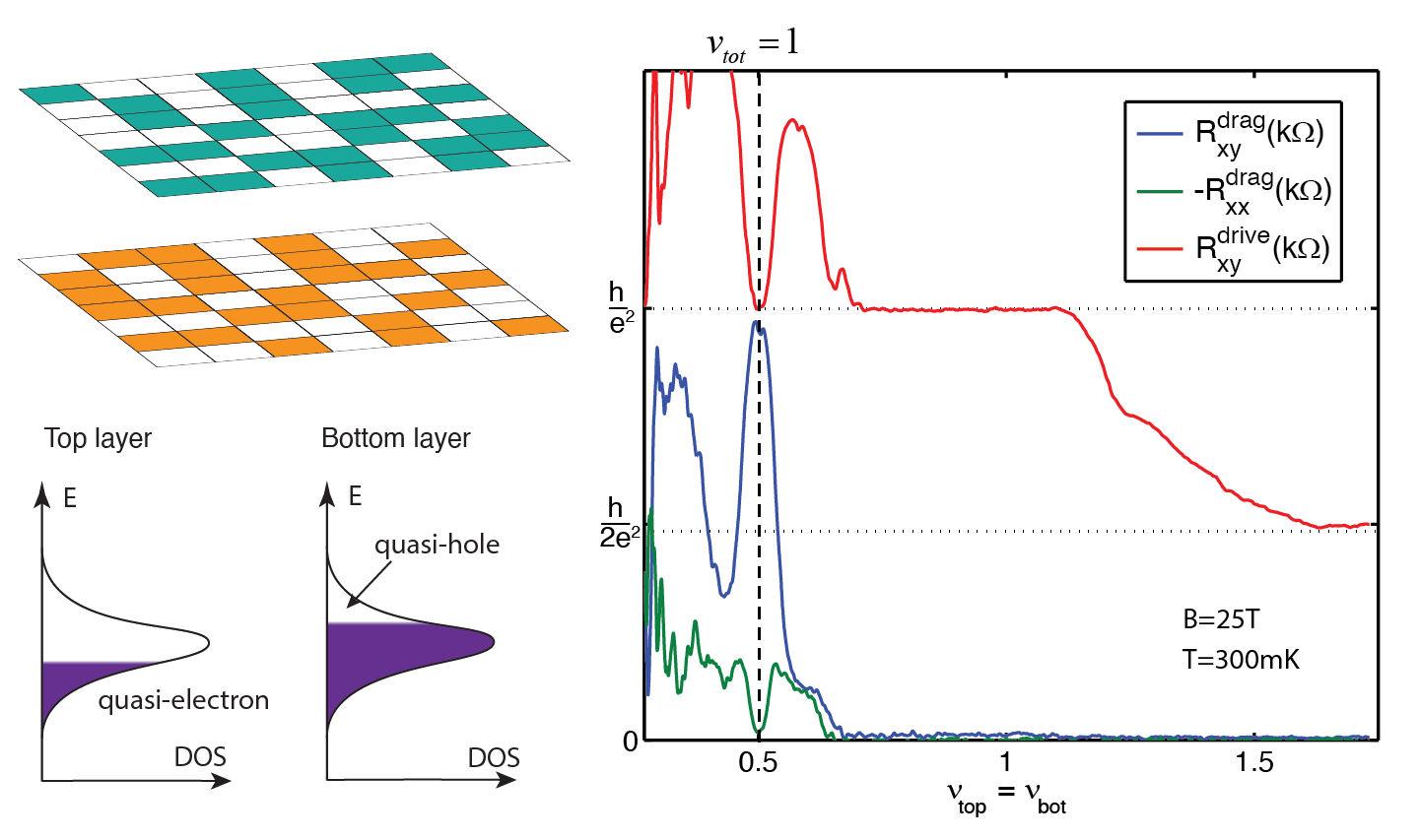
Exciton condensate in coupled Landau levels. Nature Physics (2017)

Crossover between strongly- and weakly-coupled exciton superfluid. Science (2022)

Spin polarized correlated states in a tunable flat band. Nature (2020)
Visualizing 2D Quantum Matter
As an increasing number of 2D quantum matter are discovered, the limitations of current experimental techniques become evident. Existing experiments predominantly focus on easily-accessible global measurements, leaving numerous puzzles unanswered and remarkable properties as mere conjectures. To unravel these mysteries, local probing of electron behaviors is essential. The scanning tunneling microscope (STM) is a powerful tool in this endeavor, offering atom-resolving images with the highest spatial and energy resolution among scanning probe techniques. Additionally, through scanning tunneling spectroscopy (STS), it enables the direct visualization of electron wavefunctions, providing invaluable insights into quantum matter.
Integrating STM with vdW materials is challenging, given their microscopic size, susceptibility to tip perturbations, and the propensity for surface residues from fabrication processes. Meanwhile, it also presents tremendous opportunities. The understanding of many 2D quantum matter hinges on powerful STM techniques such as STS. Moreover, by harnessing the tunability of vdW materials and exploiting the interplay between layers, we can pioneer innovative approaches to investigate insulating 2D materials, local thermodynamic and magnetic properties, transforming STM into a versatile local probe for 2D systems.
We have developed significant expertise in adapting STM to vdW materials, underscored by our success in furthering the understanding of flat bands in graphene moire materials and the fractional quantum Hall effects. We are poised to expand STM techniques to encompass broader families of vdW materials and embark on a journey to explore the strongly correlated, and topological semiconducting moire materials, elucidate the unconventional superconductivity in twisted graphene, unveil exotic quasiparticles such as anyons. Recognizing that STM exploration of 2D quantum matter is still in its infancy, we remain dedicated to the continuous innovation of novel techniques tailored for vdW materials.

STM on vdW heterostructures

Tunneling spectra of fractional quantum Hall effect. Nature Physics (2023)

Spontaneous Kekule reconstruction caused by electron correlation. Science (2022)

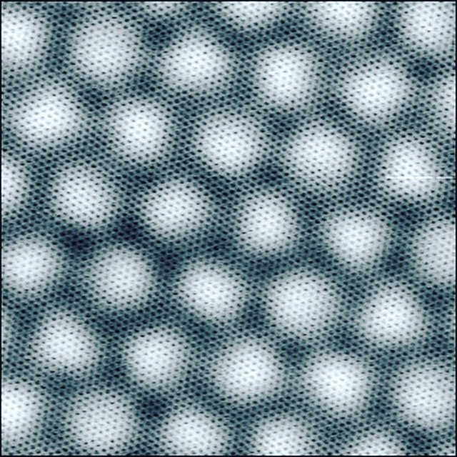
Landau orbits imaged by STM.

Innovative application of STM on vdW materials.